Back to projects
4T SRAM layout and NMOS bit-cell exploration
A transistor-level memory project comparing resistor-loaded and PMOS-loaded NMOS inverter SRAM cells, then moving toward Sky130 layout, extraction, and post-layout validation.
Build logic
What the project proves.
Architecture
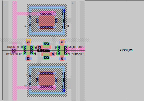
The project explores SRAM bit-cell behavior using cross-coupled NMOS inverter structures rather than a traditional CMOS 6T cell. Two access transistors connect the internal storage nodes to complementary bitlines, with the word line controlling read and write access.
Pull-up Strategy
Two pull-up approaches were compared: an explicit resistor load for early validation, and a PMOS device biased to behave like a compact pseudo-resistor. The PMOS path was important because the resistor-based layout consumed too much area for a practical tile.
Validation
Validated write speed and hold static noise margin in simulation, then planned a Magic/Sky130 layout flow with extraction and ngspice checks to understand parasitic effects after layout.
Tradeoffs
The strongest engineering value is in the constraints: balancing pull-up strength, writeability, stability, cell area, and available tool support while documenting where LTspice, xschem, and ngspice workflows differed.
Evidence
Highlights.
Compared resistor-load and PMOS pseudo-resistor NMOS inverter cells.
Documented 1.8 V operation, transistor sizing targets, speed goals, and hold SNM goals.
Used MATLAB-style butterfly-curve analysis for hold static noise margin.
Planned post-fabrication tests for read, write, and speed measurement using bitlines, word line control, and oscilloscope observation.
Next
That's a wrap.
Explore more projects or view the linked GitHub repository for full details.