Back to projects
Custom 6T SRAM bit cell, taped out
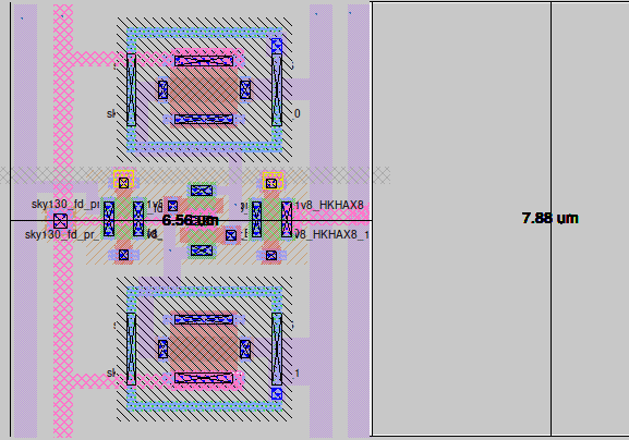
A transistor-level memory design: cross-coupled NMOS inverters with grounded-gate PMOS pseudo-resistor loads, validated in SPICE, laid out in Magic VLSI on the Sky130 130 nm process, and taped out at 51.69 µm². Silicon is due back within months.
Build logic
What the project proves.
Architecture
The cell stores its bit on cross-coupled NMOS inverters, with two NMOS access transistors connecting the internal nodes to complementary bitlines under wordline control. The pull-ups are two PMOS devices with their gates tied to ground, acting as always-on pseudo-resistors: six transistors total, but a different tradeoff space than the classic CMOS 6T.
Why grounded-gate PMOS
Two pull-up approaches were compared: an explicit resistor load for early validation, and the grounded-gate PMOS pseudo-resistor. The resistor version consumed far too much layout area for a practical tile; the PMOS load delivered the pull-up behavior in a fraction of the footprint and made the compact final cell possible.
Validation
Write speed and hold static noise margin were validated in SPICE at 1.8 V, with butterfly-curve analysis giving a 265 mV hold SNM. The layout was drawn in Magic VLSI against the Sky130 process rules, then extracted so post-layout parasitics could be checked in ngspice before submission.
Tapeout and what comes back
The final 51.69 µm² cell went out for fabrication in December 2025. When silicon returns, the bring-up plan is direct: write through the bitlines, control the wordline, and observe read behavior and speed on an oscilloscope to compare reality against simulation.
Schematic
Six transistors, one bit.
How the cell holds a bit
Two cross-coupled NMOS inverters latch the bit between nodes Q and QB. The pull-ups are PMOS devices with their gates tied to ground: always on, behaving like compact pseudo-resistors that hold the high node up without the area cost of explicit resistors.
The wordline gates two NMOS access transistors connecting Q and QB to the complementary bitlines. Drive the bitlines to write; sense them to read. Stability came down to sizing: drivers strong enough to write reliably, loads weak enough to preserve the 265 mV hold margin.
Cell schematic
Write through BL / BLB with WL high · pseudo-resistor loads hold the bit
Evidence
Highlights.
Compared explicit-resistor and grounded-gate PMOS pull-ups, choosing the PMOS pseudo-resistor for area.
Validated 1.8 V operation, write speed, and a 265 mV hold static noise margin using butterfly-curve analysis.
Completed layout, extraction, and post-layout checks with Magic VLSI and ngspice on the Sky130 process.
Taped out at 51.69 µm² in December 2025. Silicon due back for bench validation.
Next
Silicon is on the way.
The cell is out for fabrication. When the chip arrives, this page gains real measurements: read and write behavior, speed, and how post-silicon reality compares with simulation.