Back to projects
Design in progress
RF low-noise amplifier
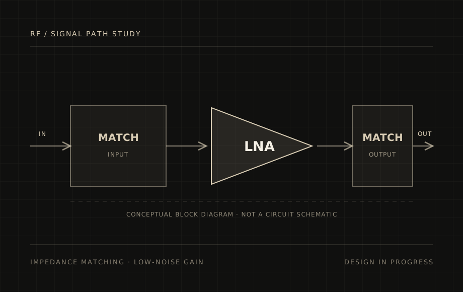
I’m developing a 1 GHz low-noise amplifier in Keysight ADS. The design targets less than 1 dB noise figure and more than 12 dB gain, with transistor biasing and stability as the current focus. Matching networks and a physical prototype follow.
Design requirements
Targets at 1 GHz
Design targets. Simulation and measured results will be added as the project progresses.
Current work
Biasing and stability
Bias network
The design is based on the Mini-Circuits SAV-541+ transistor at a bias point of 3 V and 60 mA. I’m starting with the DC feeds, blocking capacitors, and bypass network, using component S-parameter models to account for impedance and self-resonance at 1 GHz.
Stability analysis
The first design phase also covers unconditional stability from 0.1 to 2 GHz. The approach is to assess the transistor and bias network with the μ-test and stability circles, then choose output stabilization resistors while keeping track of the gain penalty.
The next design decision
Balancing noise and gain
The source impedance that gives the lowest noise figure generally differs from the one that gives the highest available gain. Selecting the input match means weighing noise against gain and return loss, while keeping the amplifier stable.
I’ll use the transistor’s noise parameters and gain circles in ADS to choose that compromise, then design the output match for maximum gain. The matching networks will begin with ideal lumped components before moving to realistic models and an EM-simulated PCB layout on 1.6 mm FR-4.
Project roadmap
Design through measurement
Biasing and stability
Characterize the passive components, develop the bias network, and assess transistor stability before selecting the matching impedances.
Noise and impedance matching
Use noise and available-gain circles to select the source impedance, then design lumped input and output matching networks against the 1 GHz targets.
Layout and fabrication
Develop the two-layer FR-4 layout with microstrip interconnects and SMA launches. Refine the circuit with EM simulation and realistic component models before preparing Gerbers and the BOM.
Assembly and RF measurements
Assemble the prototype and measure gain, noise figure, and input and output return loss. Compare the hardware against the ADS simulations and the original design targets.
More hardware
Explore another project
Custom power electronics, embedded firmware, and bench testing on DriveWire.